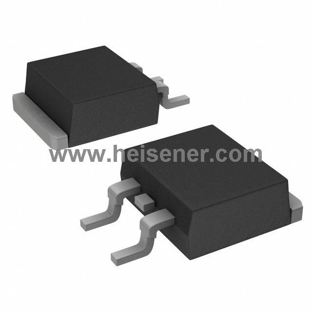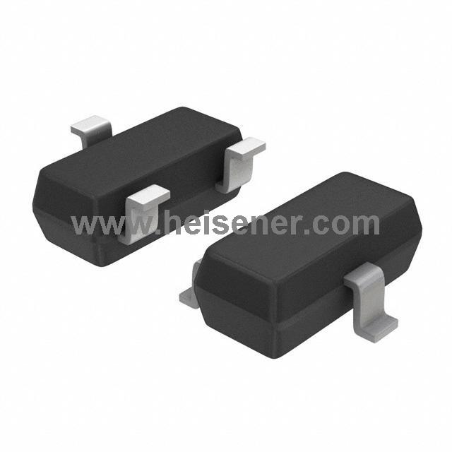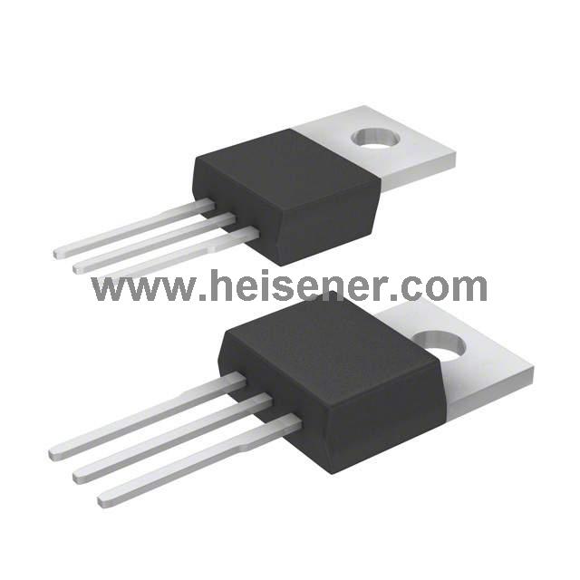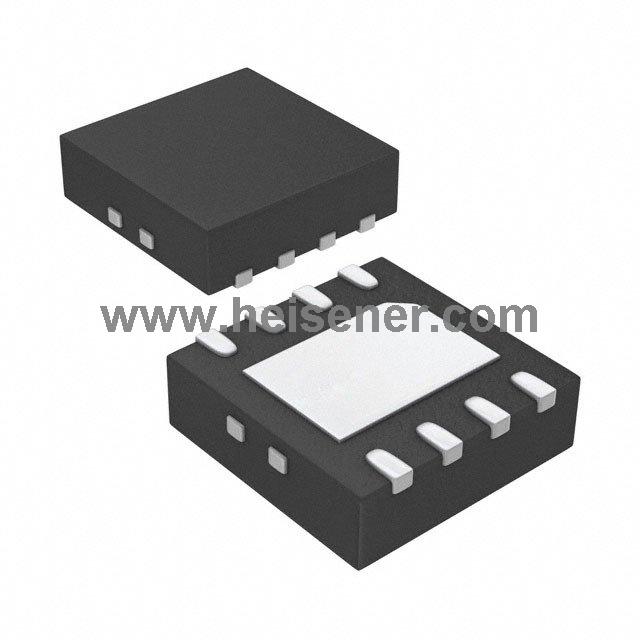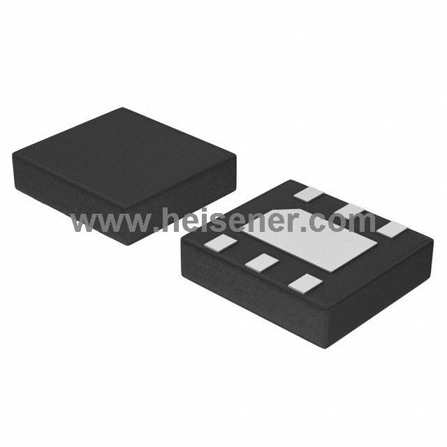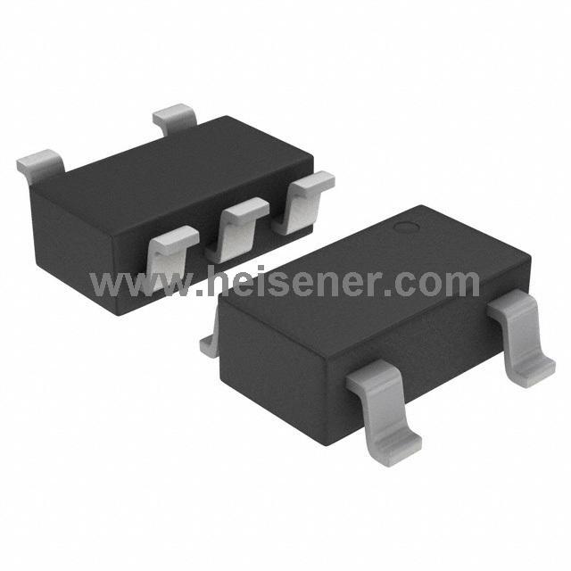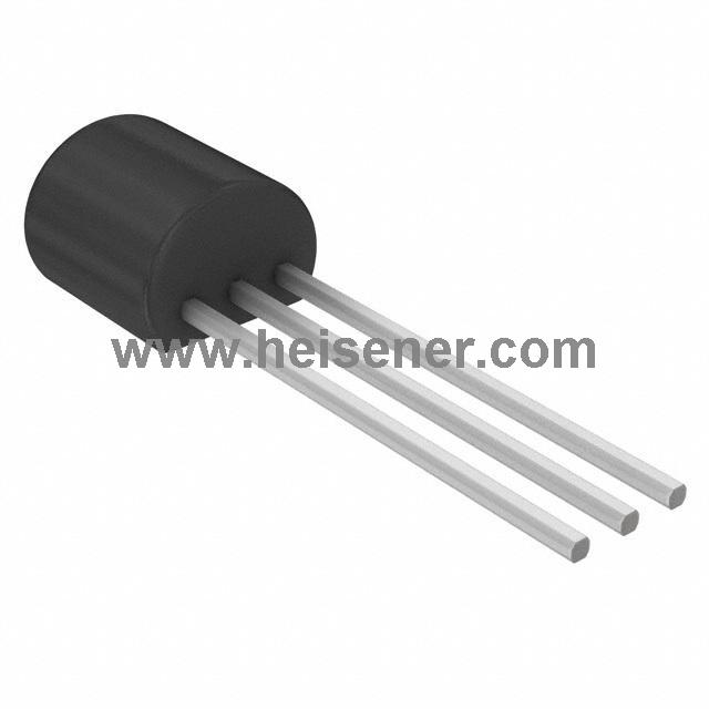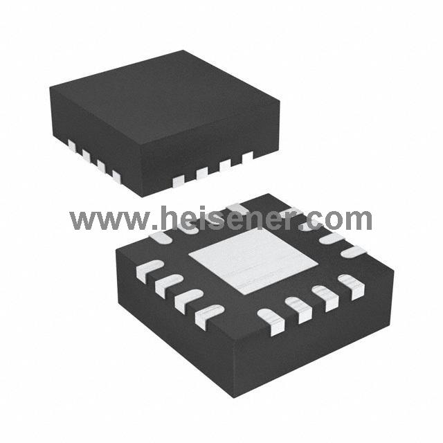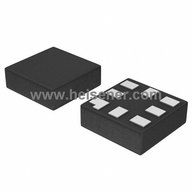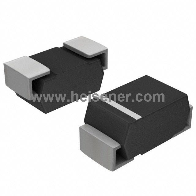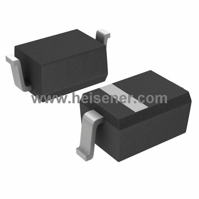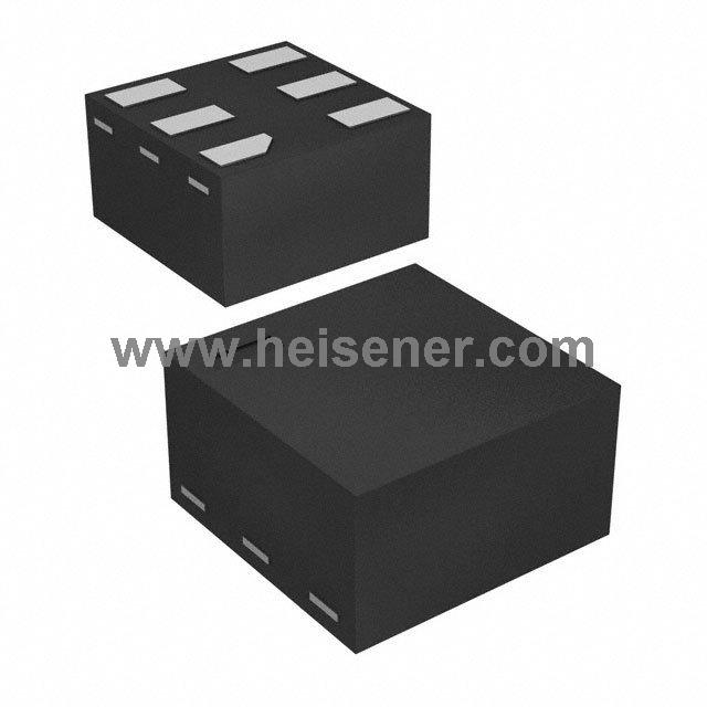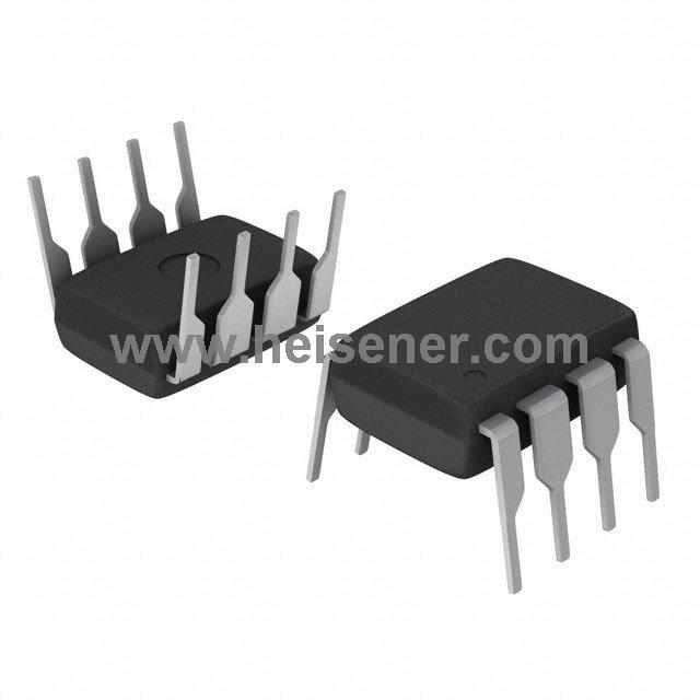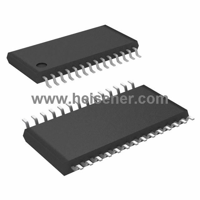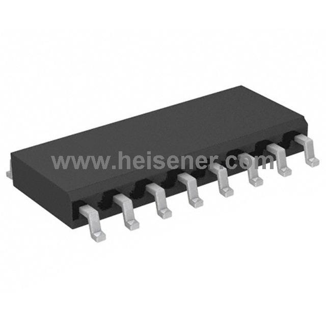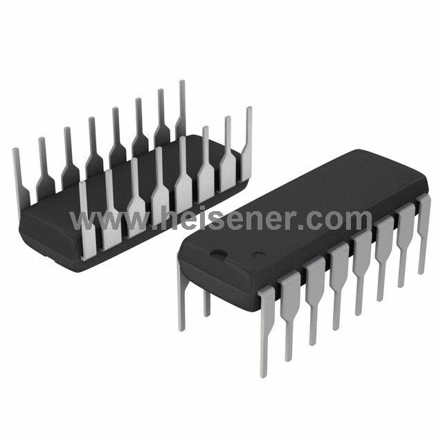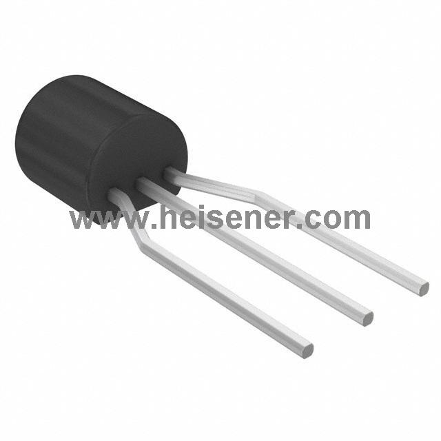
A transistor is a solid-state semiconductor device, including diodes, bipolar transistors, field-effect transistors (FETs), and thyristors. It can perform functions such as detection, rectification, amplification, switching, voltage regulation, and signal modulation.
As a controllable current switch, a transistor regulates output current based on the input voltage. Unlike mechanical switches, transistors use electrical signals to control switching operations, enabling extremely high switching speeds that can exceed 100 GHz in laboratory environments.
Early transistors were made from germanium, a semiconductor material that becomes unstable at temperatures around 80°C. Today, silicon is used almost exclusively because it can withstand temperatures of approximately 180°C.
The primary functions of a transistor are amplification and switching. For example, in a radio receiver, a transistor amplifies extremely weak radio signals so they can drive a speaker. In amplification applications, the transistor increases voltage or current without altering the signal waveform. In digital electronics, such as computers, transistors act as switches that control binary states (0 and 1), forming the foundation of digital circuits.
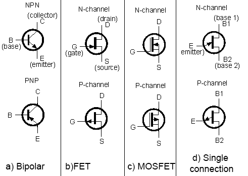
The following are the standard electrical symbols for four core types of transistors:
a) Bipolar Junction Transistor (BJT):
Available in NPN and PNP types, a BJT consists of a Base (B), Collector (C), and Emitter (E). The direction of the arrow on the emitter indicates the current flow direction—outward for NPN and inward for PNP.
b) Junction Field-Effect Transistor (JFET):
A JFET includes a Gate (G), Drain (D), and Source (S). It is available in N-channel and P-channel configurations, with the channel type identified by the direction of the gate arrow.
c) Metal-Oxide-Semiconductor Field-Effect Transistor (MOSFET):
The defining feature of a MOSFET symbol is the insulated gate, which is electrically isolated from the channel by an oxide layer. The direction of the substrate arrow distinguishes N-channel from P-channel devices. MOSFETs are the foundation of modern power electronics and switching circuits.
d) Unijunction Transistor (UJT):
A UJT consists of one Emitter (E) and two Bases (B1 and B2). It is commonly used in triggering and oscillator circuits and is available in both N-channel and P-channel versions.
A bipolar junction transistor (BJT) is constructed from differently doped semiconductor materials that create two PN junctions. Based on the doping arrangement, transistors are classified into NPN and PNP types.
A P-type transistor is created by doping silicon with trivalent elements such as boron. Since trivalent atoms have three valence electrons, their introduction into the silicon crystal creates a hole (an absence of one electron). These holes can move through the crystal lattice and carry electrical current.
An N-type transistor is created by doping silicon with pentavalent elements such as phosphorus. Pentavalent atoms have five valence electrons, and the extra electron becomes a free electron after doping. These free electrons can move through the crystal and conduct electrical current.
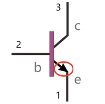
The circuit symbol of an NPN transistor is shown below. A small arrow on the emitter (E) indicates the direction of current flow.
A small control current flows from the base (B) to the emitter (E), while a larger controlled current flows from the collector (C) to the emitter (E).
The collector-emitter path conducts only when a small current is present between the base and emitter (i.e., when a voltage difference is established between them). In other words, a small base current controls a much larger collector current.
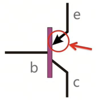
The circuit symbol of a PNP transistor is shown below. The small arrow points inward, indicating the direction of current flow.
A small control current flows from the emitter (E) to the base (B), while a larger controlled current flows from the emitter (E) to the collector (C).
The emitter-collector path conducts only when a small current exists between the emitter and base (i.e., when a voltage difference is established between them). In other words, a small emitter-base current controls a much larger emitter-collector current.
A vacuum tube is an electronic device that controls the flow of electrons in a vacuum. It operates by heating a filament to emit free electrons and uses electric fields to control and amplify the electron flow. Inside the tube, a heated filament generates electrons, while varying the voltages applied to internal electrodes controls the electron current, enabling signal amplification or rectification.
Comparison: Transistor vs. Vacuum Tube
| Feature | Transistor | Vacuum Tube |
| Size & Weight | Small, lightweight, easy to integrate | Large, heavy, less portable |
| Power Consumption | Low (mW level), low-power design | High (W level), requires warm-up |
| Switching Speed | Fast, suitable for high-frequency use | Slower due to electron inertia |
| Reliability | Long life, highly reliable | Shorter lifespan, sensitive to vibration and voltage |
| Cost | Low cost, mass-producible | Higher cost, complex manufacturing |
| Power Supply | Low-voltage DC | High-voltage DC + filament heating |
| Noise & Distortion | Low noise, low distortion | Higher noise, but valued for "warm" audio tone |
| Main Applications | Digital circuits, microprocessors, high-speed systems | Analog amplification, audio, radio communication |
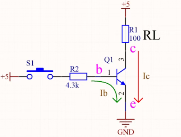
NPN Transistor
When switch S1 is pressed, about 1 mA of base current (Ib) flows through the transistor, driving it into saturation. The collector-emitter path is fully turned on, and the collector voltage drops close to 0 V (GND). The voltage across the load RL is approximately 5 V.
Both Ib and Ic flow into the emitter, so the emitter is at low potential and should be connected to ground. The collector is connected to the load and the power supply.
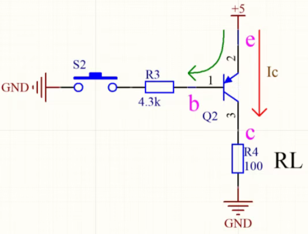
PNP Transistor
When switch S2 is pressed, about 1 mA of base current (Ib) flows through the transistor, driving it into saturation. The emitter-collector path is fully turned on, and the collector voltage rises close to 5 V. The voltage across the load RL is approximately 5 V.
Both Ib and Ic flow out of the emitter, so the emitter is at a high potential and should be connected to the power supply. The collector is connected to the load and ground.
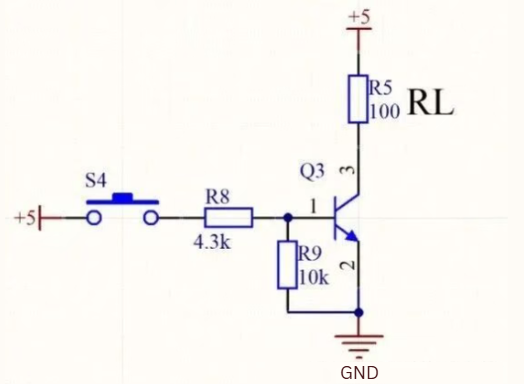
NPN Transistor with a Pull-Down Resistor
For an NPN transistor, a pull-down resistor is typically added at the base. It helps discharge the base-emitter capacitance faster, improving turn-off speed. It also ensures a defined logic state at the base, preventing unstable operation when the control input is floating or in a high-impedance state.
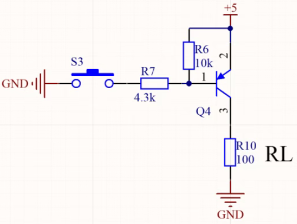
PNP Transistor with a Pull-Up Resistor
For a PNP transistor, a pull-up resistor should be added at the base, following the same principle as above.
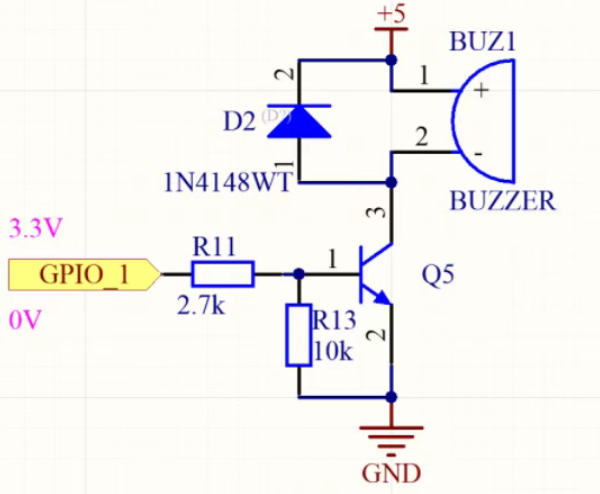
Driving a Buzzer with an NPN Transistor
For inductive loads, a reverse flyback diode must be connected in parallel across the load. When the transistor turns off, the coil generates a high reverse electromotive force due to self-induction. The flyback diode provides a freewheeling path for the current and clamps the reverse voltage, preventing transistor breakdown. The diode should be a fast-recovery diode or a Schottky diode, as both offer fast switching speed.
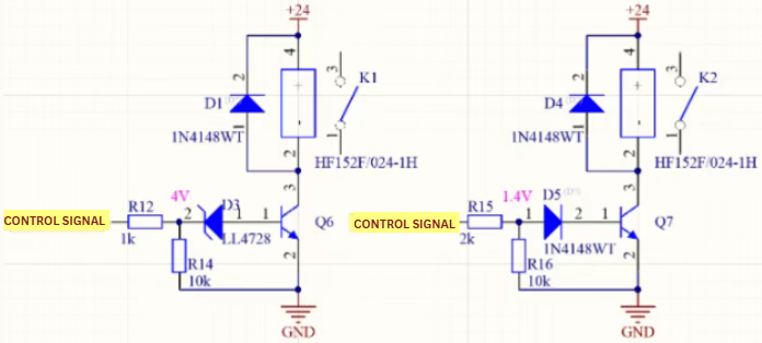
Driving a Relay with an NPN Transistor
For some control signals, the low level may not be a true 0 V and is typically within 1 V. To ensure the transistor is fully turned off, a reverse Zener diode or a forward diode is often added at the base to increase the turn-on threshold voltage of the transistor.
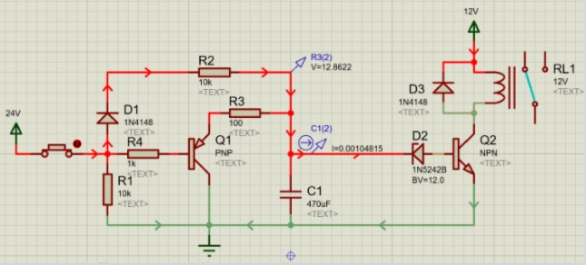
Delay Control of a Relay with a Transistor
This is a simulation circuit for delayed turn-on and fast turn-off of a transistor. D1, R2, C1, and D2 form the delay turn-on path for Q2. When the voltage on C1 reaches 12 V, Q2 turns on. R3, Q1, R4, and R1 form the fast turn-off path for Q2, where C1 is quickly discharged through R3 and Q1.
In electronic circuits and repair, correctly identifying transistors and understanding their parameters is a fundamental skill. The following sections introduce testing methods for transistors.
1. Identifying the Base and Transistor Type
Set the multimeter to the resistance range R×100 (or R×1K). First, connect the red probe to one pin and the black probe to another to measure a resistance value. Then keep the red probe on a different pin and repeat the measurement. After testing all combinations three times, identify the pair that shows two very low resistance readings. The pin connected to the red probe in this case is the base, and the transistor is a PNP type.
Conversely, if the black probe is used as the reference and the same condition is found (two low resistance readings), then the pin connected to the black probe is the base, and the transistor is an NPN type.
2. Identifying the Collector
A transistor has higher current gain (β) when the emitter and collector are correctly connected, resulting in a larger meter deflection. When reversed, β becomes much smaller.
First, assume one pin as the collector. For an NPN transistor, connect the emitter to the black probe and the assumed collector to the red probe. During measurement, hold the base and the assumed collector with your fingers (without letting them touch). If the meter shows a large deflection, and the deflection becomes much smaller after swapping the two pins, the assumption is correct. This confirms the collector and emitter.
3. Estimating Current Gain (β)
Set the multimeter to R×100 (or R×1K). For an NPN transistor, connect the red probe to the emitter and the black probe to the collector. Compare two cases: holding the base and collector together with your fingers versus releasing them. A larger change in meter deflection indicates a higher β value.
The main types include BJT (NPN/PNP), JFET, MOSFET, and UJT, with BJTs and MOSFETs being the most commonly used.
A transistor uses a small base current to control a larger collector-emitter current, enabling fast ON/OFF switching in electronic circuits.
It protects the transistor from high reverse voltage generated by inductive loads when switching off, by providing a safe current path.
By measuring resistance combinations with a multimeter and identifying the pin that shows two low-resistance readings as the base.
Transistors are smaller, faster, lower power, and more reliable, while vacuum tubes are larger, higher power, and mainly used in analog or audio applications.