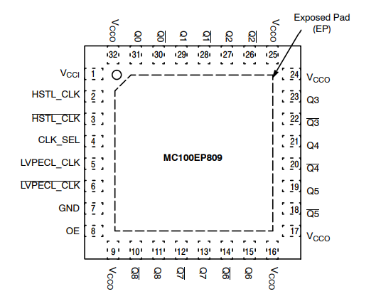
MC100EP809 is a low-bias 2:1:9 differential clock driver. The clock distribution is considered in the design, and two clock sources are accepted into the input multiplexer. This component is designed for low voltage applications and requires a large number of outputs to drive accurately aligned low tilt signals to the destination.
Logic Diagram
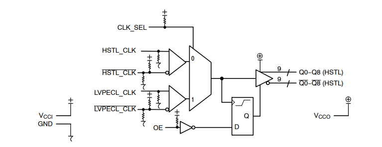
The two clock inputs are a differential HSTL and a differential LVPECL. Both input pairs can accept LVDS level. They are made by CLK_ SEL pin (LVTTL) selected. In order to avoid generating weak clock pulses when the device is enabled/disabled, the output enable (OE), namely LVTTL, is synchronous, and ensure that the output is enabled/disabled only when it is in the LOW state.

Output Enable (OE) Timing Diagram
MC100EP809 guarantees low output-to-output tilt. The optimized design, layout and processing minimize the inclination within the equipment and between batches. The MC100EP809 output structure adopts an open emitter structure and will terminate with 50 pairs of ground instead of the standard HSTL configuration

Output termination and AC test reference
In order to ensure the realization of tight tilt specification, even if only one output is used, both ends of the differential output need to be equally terminated at 50. If one output pair is not used, both outputs can remain open (not terminated) without affecting skew. Designers can use the performance of EP809 to distribute the low-tilt clock on the backplane. Both clock inputs can be biased single-ended driven by the non-drive pin in the input alignment
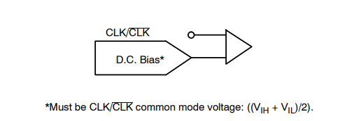
Single-ended CLK/CLK input configuration
Features
● 100 ps Typical Device−to−Device Skew. 100 ps typical device −to−Device skew
● 15 ps Typical within Device Skew
● HSTL Compatible Outputs Drive 50 to GND with no Offset Voltage
● Maximum Frequency > 750 MHz
● 850 ps Typical Propagation Delay
● Fully Compatible with Micrel SY89809L
● PECL and HSTL Mode Operating Range: VCCI = 3 V to 3.6 V with GND = 0 V, VCCO = 1.6V to 2.0V
● Open Input Default State
● This Device is Pb−Free and is RoHS Compliant