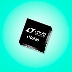
To enable battery-powered, high-performance broadband transmitters to operate in the 700MHz to 6GHz range, Linear Technology Corporation has introduced a new low-power I / Q modulator, the LTC5589. The company said that with a single 2.7V to 3.6V power supply, the LTC5589 consumes only 29.5mA, which is a 50% reduction in power consumption over other solutions.
The new modulator features best-in-class -50dBc sideband rejection and -43dBm (typical, uncalibrated) carrier leakage. Using the on-chip tuning function through the SPI bus can further improve sideband and carrier rejection, which are better than -60dBc and -60dBm, respectively. In addition, the output noise floor of this device is very low, -158.8dBm / Hz, plus OIP3 of 19dBm, which has excellent transmitter performance.
The LTC5589 supports narrowband and wideband transmitters. Its baseband bandwidth is extended to 92MHz, gain flatness is ± 1dB, and it provides an RF bandwidth of 184MHz at 1.8GHz. Combined with low power consumption and powerful performance, the device is suitable for a variety of demanding applications in radio and wireless communications. These include broadband modems, femtocell and picocell broadband wireless access, wireless microphones and portable audio systems, broadband portable field radios, unlicensed band radios, train communications, software-defined radios, portable RF test equipment, low-power microwave backhaul And repeaters, telemetry radios and satellite modems.
Existing zero-IF modulators exhibit excessive carrier leakage and poor sideband suppression, resulting in poor error vector magnitude (EVM) and adjacent channel power ratio (ACPR). Calibration is challenging, and it relies on digital tuning algorithms in a baseband FPGA using an external DAC. Adjusting the resolution is usually limited. The LTC5589 provides on-chip tuning capabilities for phase and amplitude mismatch of the I and Q channels, which affects sideband rejection. The device also has a DC offset balance adjustment function, which will affect carrier leakage. With built-in serial port controlled calibration, the LTC5589 simplifies calibration and is cost effective.
The gain of the LTC5589 can be set through the on-chip serial port. The coarse gain control provides 1dB / step, and the adjustable fine gain control is 0.1dB. The total gain range is -19dB to 0dB. Modulator gain changes affect device supply currents from 9mA to 39mA, so the device can be set to lower power consumption and slightly reduce gain and performance based on the needs of a particular application. After setting, the gain can be automatically compensated by activating the on-chip temperature correction function.
The LTC5589 is packaged in a 4mm x 4mm plastic QFN to provide a smaller solution footprint. The specified operating temperature range is -40 ° C to 105 ° C. The device has an enable pin for TDD or burst mode transmitter operation. When disabled, the LTC5589 saves power by drawing a standby current of typically 0.6µA. The modulator can be turned on with full quadrature accuracy within 350ns.
