The IRF540 MOSFET series uses STMicroelectronics' unique STripFET process to minimize input capacitance and gate charge. This design makes the IRF540 particularly well-suited as the primary switch in advanced, high-efficiency, high-frequency isolated DC-DC converters for telecom and computer applications. Additionally, this MOSFET is ideal for any application with low gate drive requirements. The optimized characteristics of the IRF540 not only enhance switching performance but also reduce energy loss, making it a popular choice for high-performance electronic systems.

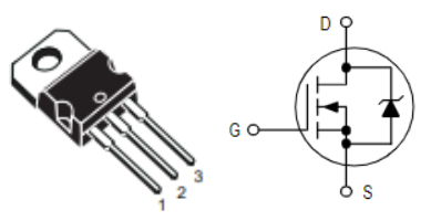
The pins of IRF540 are as follows:
D (Drain): Current flows through here when the MOSFET is on.
G (Gate): Controls the MOSFET’s switching.
S (Source): Current exits through this pin; usually connected to ground.


Unclamped Inductive Load Test Circuit

Unclamped Inductive Waveform

Switching Times Test Circuits For Resistive Load

Gate Charge test Circuit

Test Circuit For Inductive Load Switching And Diode Recovery Times
Parameter
|
Value
|
Drain-Source Voltage (Vds)
|
100V
|
Gate-Source Voltage (Vgs)
|
±20V
|
Drive Voltage (Max Rds On, Min Rds On)
|
10V
|
Current - Continuous Drain (Id) @ 25°C
|
22A (Tc)
|
Pulsed Drain Current (Id)
|
110A
|
Rds(on)
|
0.044Ω
|
Rds On (Max) @ Id, Vgs
|
77mOhm @ 11A, 10V
|
Vgs(th) (Max) @ Id
|
4V @ 250µA
|
Gate Charge (Qg) (Max) @ Vgs
|
41 nC @ 10 V
|
Input Capacitance (Ciss) (Max) @ Vds
|
870 pF @ 25 V
|
Power Dissipation (Max)
|
85W (Tc)
|
Operating Temperature Range
|
-55°C - 175°C
|
Total Gate Charge (Qg)
|
67 nC
|
Rise Time (tr)
|
52 ns
|
Fall Time (tf)
|
45 ns
|
Package Type
|
TO-220
|
IRF540 Features
Typical RDS(on) = 0.055Ω
Exceptional dv/dt Capability
100% Avalanche Tested
Low Gate Charge
Application Orientedo
Diode is Characterized for Use in Bridge Circuits
IDSS and VDS(on) Specified at Elevated Temperature
Repetitive Avalanche Rated
Fast Switching
Ease of Paralleling
Simple Drive Requirements
IRF540 Applications
High-efficiency DC-DC Converters
UPS and Motor Control
Power Supplies
Bridge Circuits
Telecommunication Equipment
Computer Hardware
Battery Management Systems
IRF540 Package
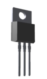
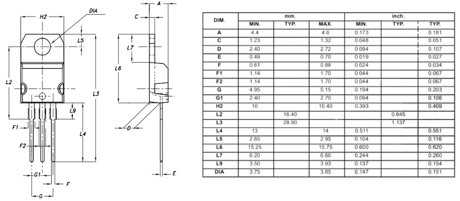
The IRF540 MOSFET is housed in a TO-220 package, which is a standard and widely used package for power transistors. This package is known for its excellent thermal dissipation properties, making it suitable for high-power applications. The TO-220 package features three pins—drain,a gate, and source—arranged for easy mounting on a PCB or heat sink.
 FAQs
FAQsWhat is the IRF540 MOSFET used for?
The IRF540 is commonly used in power supplies, motor control circuits, DC-DC converters, and switching applications.
Is the IRF540 suitable for logic-level drive?
No, the IRF540 is not a logic-level MOSFET, so it requires a higher gate drive voltage, typically around 10V, for optimal switching.
What is the typical turn-on and turn-off time of the IRF540?
The typical turn-on time is 35ns, and the turn-off time is around 67ns, which makes it suitable for fast switching applications.
What are some alternatives to the IRF540?
Some alternatives to the IRF540 include the IRF640, IRF530, STP55NF06, and more.